The MAX74811ARMZ-R7 is a dual-channel, auto-zero amplifier optimized for low-offset, low-drift precision signal chains; the datasheet highlights a ≤1 µV offset, 2.5 MHz gain-bandwidth product, 1 V/µs slew rate, and a 2.7–5.5 V single-supply range, which make it suitable for sensor front-ends and ADC drivers. Engineers consult the datasheet and pinout early to match device limits to system requirements. The published electrical tables provide typical vs. maximum columns for Vos, Ib, PSRR, and CMRR that guide design margining. Use those table conditions (temp, supply, load) to derive expected in-circuit performance before PCB layout and prototype testing.
Product Overview and Key Features
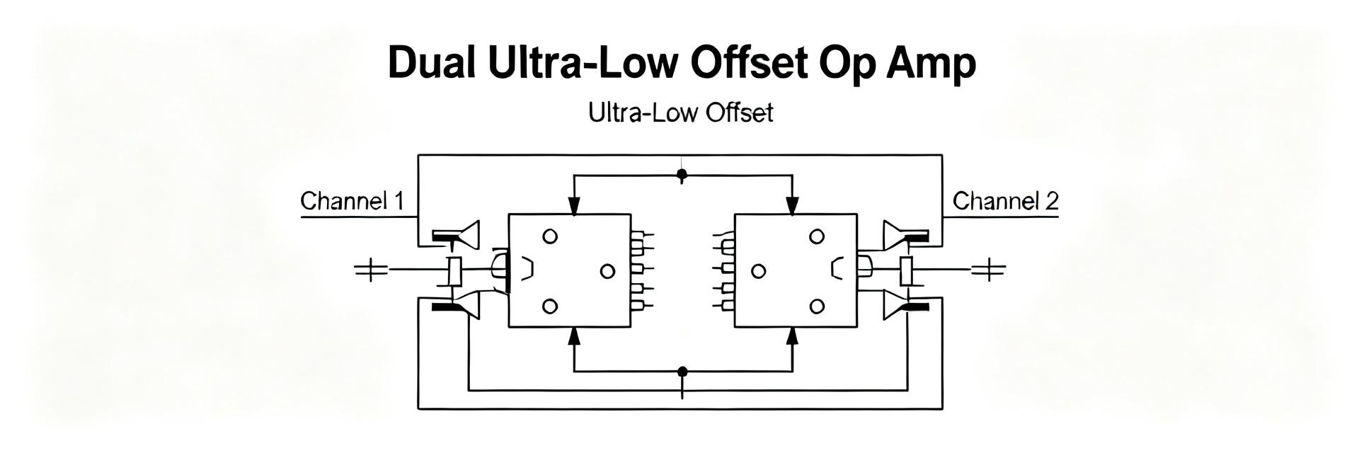
1.1 What the MAX74811ARMZ-R7 Is
The MAX74811ARMZ-R7 is a dual-channel chopper (auto-zero) op amp providing ultralow input offset and rail-to-rail I/O on a single 2.7–5.5 V supply. Datasheet DC and AC summary rows show ≤1 µV offset, ≤30 pA input bias, and a 2.5 MHz GBP. Those specs translate to sub-microvolt drift in precision sensors and predictable closed-loop bandwidth for modest gains, making it a strong choice for low-noise instrumentation.
1.2 Quick Comparison (where it fits in designs)
Compared to general-purpose op amps, this device trades bandwidth and drive for offset performance and low bias. Typical supply current and GBP are lower than high-speed op amps, while offset and bias are orders of magnitude better. Use it when offset and drift dominate error budget (e.g., bridge sensors, thermopiles), but avoid for high-speed buffering where MHz-level closed-loop bandwidths are required.
| Specification | Value / Range | Conditions / Note |
|---|---|---|
| Input Offset Voltage (Vos) | ≤ 1 µV (max) | At TA = 25°C |
| Gain-Bandwidth Product (GBP) | 2.5 MHz | Typical |
| Slew Rate (SR) | 1 V/µs | Typical |
| Supply Voltage Range (V+) | 2.7 V to 5.5 V | Single-supply configuration |
| Input Bias Current (Ib) | ≤ 30 pA | Ultralow leakage |
| Package Type | MSOP-8 | Compact footprint |
Pinout & Package Details
2.1 Pin-by-pin Explanation (MSOP-8)
Correct pin connections prevent common mistakes and ensure ratings are respected. The MSOP-8 pin map lists V+ (supply), GND, IN+, IN–, OUT for channels A and B, plus any NC/substrate pins. Typical pin assignments: 1 = OUTA, 2 = IN–A, 3 = IN+ A, 4 = GND, 5 = IN+ B, 6 = IN–B, 7 = OUTB, 8 = V+ (verify in the datasheet). Leave NC as recommended and tie substrate per manufacturer notes to avoid leakage; consult the pinout when placing decoupling and guard traces.
2.2 Package Mechanical & Thermal Notes
Mechanical drawing and thermal metrics constrain footprint and thermal design. The datasheet gives MSOP-8 dimensions and θJA; recommended land patterns include thermal vias when applicable. For low-power parts thermal vias may be optional, but place the 0.1 μF decoupling within 1 mm of V+ pin, follow recommended solder mask openings, and respect clearance for high-impedance nodes to minimize contamination and leakage.
Electrical Characteristics & Performance Data Deep-Dive
3.1 DC Specs to Watch (offsets, bias, supply)
DC parameters set the baseline error and operational limits. Key table entries include Vos (typical and max), input bias current, supply current, common-mode range, and output swing to rails. Read measurement conditions carefully—temperature and supply used for typical columns matter; margin Vos by expected temperature drift and account for bias current in high-source-impedance sensor interfaces with guard traces or input buffers.
3.2 AC/Transient Specs (GBP, SR, noise)
AC specs determine closed-loop bandwidth and transient response. GBP is 2.5 MHz and slew rate 1 V/µs; input-referred noise figures and phase margin notes appear in AC tables. Estimate closed-loop bandwidth as GBP divided by closed-loop gain (for example, at gain = 10, fc ≈ 2.5 MHz / 10 ≈ 250 kHz), and check slew-limited settling for large steps; add feedback compensation or limit bandwidth if driving capacitive loads.
Typical Application Circuits & Design Guidelines
4.1 Example Circuits (sensor front-end, buffer, low-pass filter)
Typical applications show how the device’s low offset improves overall system error. Datasheet application examples include an ADC driver buffer, single-supply noninverting sensor amplifier, and a simple RC low-pass at the output. For ADC buffering use a noninverting buffer with a small feedback capacitor (pF-range) to control peaking; for bridge sensors place a low-value input resistor to limit input currents while preserving low offset contribution.
4.2 Component Selection & Stability Tips
Component choices and compensation keep the amplifier stable under real loads. Notes in application sections warn about capacitive loads, recommended series output resistor, and feedback capacitors. Add a 10–50 Ω series resistor when driving cables or ADC inputs with sampling capacitors; use feedback capacitors (10–100 pF) in high-gain configs to preserve phase margin and reduce overshoot.
PCB Layout, Testing & Troubleshooting Checklist
5.1 PCB Layout & Decoupling Best Practices
Layout directly affects noise and offset behavior referenced to the pinout. Layout recommendations specify 0.1 μF decoupling close to V+, short return paths, and ground plane use. Place decoupling within 1 mm of V+ pin, use a solid ground plane, keep high-impedance inputs short, and implement guard rings for ultra-low bias circuits; follow the pinout when routing to avoid cross-talk and leakage.
5.2 Test Procedures & Common Failure Modes
A concise test checklist reduces debug time. Typical checks include power-up current, offset at 25°C, frequency sweep for bandwidth, step response, and load testing. If excessive offset appears, check contamination, flux residues, or leakage paths; verify supply decoupling and probe loading (use high-impedance or differential probes). Common fixes: clean board, add guarding, or adjust input network.
Key Summary
- The MAX74811ARMZ-R7 delivers ultralow offset and low bias current ideal for precision sensor front-ends; consult the datasheet tables for Vos and Ib to size input networks.
- Follow the MSOP-8 pinout strictly: place decoupling within 1 mm of V+, keep analog inputs short, and guard high-impedance nodes to minimize leakage and drift.
- Use GBP/divide-by-gain to estimate closed-loop bandwidth (e.g., gain=10 → ~250 kHz) and add feedback capacitance or series output resistor for stability with capacitive loads.
Frequently Asked Questions
What are typical Vos and drift values for the MAX74811ARMZ-R7?
Typical Vos is listed as ≤1 µV in the datasheet under specified conditions, with low drift across temperature. Measure offset at 25°C with shorted inputs and a stable supply; if drift is higher, inspect layout contamination, add guarding, or tighten thermal coupling.
How should the MAX74811ARMZ-R7 pinout be wired for a single-supply buffer?
Wire V+ to the supply pin with a 0.1 μF decoupling cap close to the pin and connect GND to the ground pin; configure the channel as a unity-gain buffer by tying OUT to IN– and feeding IN+ from the signal source. Ensure inputs see valid common-mode range per the datasheet.
What test steps verify MAX74811ARMZ-R7 closed-loop bandwidth and slew response?
Apply a small-amplitude sine sweep through the closed-loop gain and measure gain vs frequency to find the –3 dB point; for slew, apply a large step and measure slew-limited slope. Use low-capacitance probes and validate against datasheet AC/transient columns.
What decoupling capacitor layout is recommended for the MAX74811ARMZ-R7?
Place a 0.1 μF ceramic decoupling capacitor within 1 mm of the V+ pin directly to a solid, low-impedance ground plane. This minimizes high-frequency noise and prevents oscillation in the high-gain amplifier.




