A compact, practical reference for engineers and designers.
The LF347N is a quad J‑FET input operational amplifier with a typical gain‑bandwidth product near 3 MHz, a slew rate around 13 V/µs, input bias currents in the picoampere range, and a wide supply range of ±3 V to ±18 V. This article turns the LF347 datasheet into a compact, practical reference for engineers: it explains the pinout, highlights the critical electrical specs to memorize, and gives quick bench tests designers can run before committing the part to a board.
Background & Key Specs (background introduction)
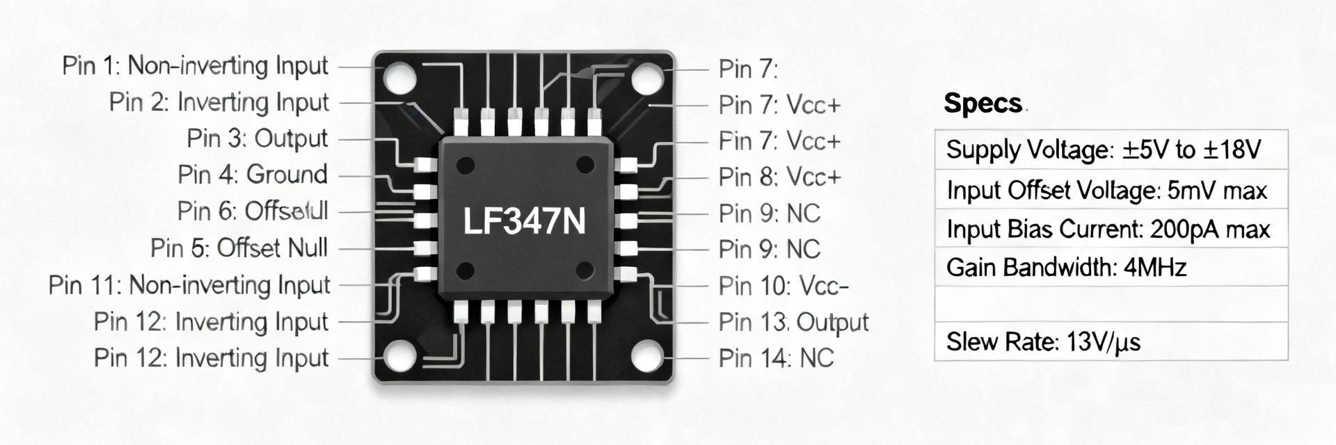
What the LF347N is — functional summary and typical applications
The LF347N is a quad J‑FET‑input amplifier intended for analog signal conditioning where low input current and moderate bandwidth are required. Typical use cases include unity‑gain buffers, integrators, DAC output drivers, and sample‑and‑hold front ends. Designers choose it for low input leakage, moderate slew and GBW, and low supply current compared with older bipolar quads—making it a practical choice where rail‑to‑rail operation is not required.
Headline datasheet numbers to remember
- Input common‑mode range and output swing: does not reach rails—expect output several volts from rails under load.
- Input capacitance and noise: modest input capacitance (few pF) and low to moderate voltage noise—suitable for many precision analog front ends but not ultra‑low‑noise RF use.
LF347N Pinout & Functional Pins (case / pinout focus)
Standard 14‑pin DIP/SOIC pin mapping (pin‑by‑pin)
Typical 14‑pin quad op amp arrangements map two rails, four inputs/inverting, four inputs/non‑inverting, four outputs, and any offset‑null pins across the package. In practice verify pin orientation on the specific package: common pitfalls are reversed supply rails and swapped inverting/non‑inverting pins when reflowing or hand‑placing the device. On board checks should include correct V+ and V‑ orientation, correct grouping of each amplifier's +/‑ inputs with its output, and confirming unused pins are not left floating.
Package variants and footprint notes
The part is commonly available in PDIP and SOIC packages; mechanical checks matter: SOIC pin spacing and body width differ from PDIP, and lead‑bend orientation changes pin numbering by package. No special thermal pad is required, but ensure solder fillets on SOIC pads and confirm pin‑1 orientation via the notch or dot. For multi‑op‑amp packages, keep sensitive inputs short and avoid routing sensitive traces under the body to minimize leakage and crosstalk.
Electrical Characteristics & What They Mean for Your Circuit (data analysis)
DC parameters to watch in designs
Input offset, input bias/current, and input‑offset drift directly set DC accuracy. Example: in a gain‑of‑100 noninverting amplifier, a 3 mV input offset produces ~0.3 V error at the output (3 mV × 100 = 300 mV). Budget this against ADC range and consider offset trim or calibration if error is unacceptable. Input bias currents flowing through large source resistances create additional voltage errors; keep source resistances low or use input bias compensation where needed.
AC and dynamic specs: bandwidth, slew, stability
Use GBW to estimate closed‑loop bandwidth: BW ≈ GBW / gain. Example: with GBW ≈ 3 MHz and gain of 10, expect ≈300 kHz bandwidth. For large amplitude signals, slew rate limits maximum undistorted sine amplitude: fmax ≈ SR / (2π·Vpk). With SR ≈ 13 V/µs and Vpk = 10 V, fmax ≈ 206 kHz.
Design & Troubleshooting Checklist (actionable guidance)
When to Use/Avoid
Good fit: applications needing low input current, moderate bandwidth, and low quiescent current.
Avoid: when rail‑to‑rail I/O, very high GBW, or single‑supply low‑voltage operation is required. Prioritize GBW and SR in datasheets when comparing alternatives.
Common Issues & Fixes
- Oscillation: Add local feedback compensation or improve decoupling.
- Excessive Drift: Check leakage paths, clean flux, or add offset trim.
- Crosstalk: Separate sensitive inputs, use ground pours/guard rings.
PCB Layout & Decoupling Best Practices (method / implementation)
Power decoupling and grounding tips
Place a 0.1 µF ceramic decoupling capacitor as close as possible to the supply pins of the package, with short traces to the pins and a nearby 10 µF bulk capacitor. Good ground practice—single point or quiet analog ground—reduces noise and prevents oscillation. Decoupling close to each amplifier section is effective; poor decoupling commonly causes unintended peaking or oscillation in moderate‑GBW devices.
Routing and input protection
Keep input traces short and avoid routing high‑impedance nodes near noisy or digital signals. For very small bias currents, consider guard rings or driven shields tied to the input reference to minimize leakage. Add series resistors for stability with capacitive loads and consider input protection (series resistor + clamp) for boards that undergo testing or ESD exposure.
Conclusion
The LF347N offers a practical combination of low input current, modest GBW (~3 MHz), and a healthy slew rate (~13 V/µs) for a wide range of analog tasks where rail‑to‑rail behavior is unnecessary. Keep the highlighted spec numbers and the simple bench tests in your toolbox, and apply the layout and decoupling tips before committing the part to production to avoid common failures and performance surprises.
Key Summary
- Memorize Specs: GBW ≈ 3 MHz, SR ≈ 13 V/µs, input bias in pA range, supply ±3 V to ±18 V.
- Quick Checks: Unity‑gain buffer, DC offset, and slew test validate functionality in minutes.
- PCB Rules: 0.1 µF decoupling close to pins, short input traces, and guard techniques for high‑impedance nodes.
FAQ
How do I verify LF347 datasheet gain‑bandwidth on the bench?
Configure a closed‑loop gain (for example, gain = 10), drive with a small‑signal sine, and sweep frequency until the output drops by 3 dB. The closed‑loop −3 dB point multiplied by the closed‑loop gain approximates the device GBW. Use low amplitude to avoid slew limitations.
What test setup gives a reliable LF347N slew rate measurement?
Use a pulse source with fast edges and amplitude within the device supply headroom; observe the output step on a scope with sufficient bandwidth. Measure the slope during the linear portion of the transition (dV/dt). Ensure the input step is large enough to exceed small‑signal response but not so large that output saturates against the rails.
How should I check LF347 pinout 14‑pin DIP orientation on a populated board?
Confirm package marking (notch or dot) for pin‑1, verify power rails with the device unpowered using continuity to ground/power planes, and visually trace each amplifier’s input/output pins to their circuit nodes. If in doubt, remove the device and check pin mapping against the verified board footprint before reflowing.




