The INA187A3IDBVR datasheet specifies a wide common-mode range of −2 V to 42 V, low input-bias behavior, and a small-signal bandwidth on the order of hundreds of kilohertz, making it optimal for precision bidirectional current-sensing. Translating static spec tables into testable, physical bench metrics is critical to secure robust engineering margins and prevent field failures. This article analyzes the datasheet limits, explores hardware failure modes, and establishes validation guidelines for system-level current sense design.
1 — Background: Device Purpose & System Role
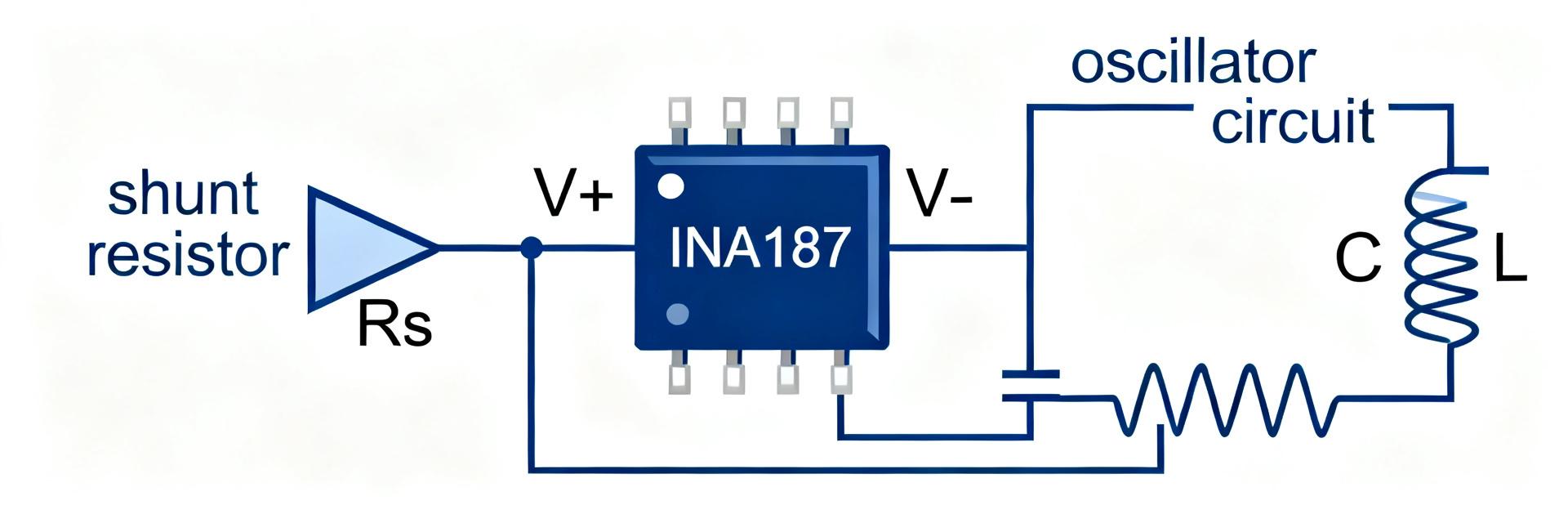
Target Application & Functional Topology
The INA187A3IDBVR is a bidirectional, zero-drift, voltage-output current-sense amplifier. It is designed to sense the differential voltage drop across a shunt resistor placed in paths with high-voltage transients. Whether deployed in high-side rail monitoring or low-side return paths, the device converts a small shunt voltage ($V_{SENSE}$) into a ground-referenced output signal scaled by a fixed gain of 100 V/V. This high gain simplifies interface connections to downstream SAR or Sigma-Delta ADCs.
Key Datasheet Parameters to Extract
Before schematic capture, designers must extract critical parameters from the datasheet to construct a system error budget:
- Common-Mode Voltage ($V_{CM}$): −2 V to 42 V (continuous operation without damage).
- Input Offset Voltage ($V_{OS}$): ±10 µV (typ), ±80 µV (max over temp) ensuring precision at low currents.
- Gain Error: ±0.2% maximum, defining the slope accuracy of the transfer curve.
- Input Bias Current ($I_{IB}$): 15 µA (typ) at high common-mode, which affects external input filter matching.
- Output Voltage Swing ($V_{OL}$ / $V_{OH}$): Determines the lowest and highest measurable current limits.
2 — Electrical Specs Deep-Dive: DC & Quasi-Static Performance
Input-Level Specifications: Offsets, Bias, & Common-Mode
The accuracy of low-current measurements is dominated by the input offset voltage ($V_{OS}$) and input bias current ($I_{IB}$). The measured input-referred current error is calculated using the following model:
I_error = [ V_OS + (I_IB_plus × R_F1) − (I_IB_minus × R_F2) ] / R_SHUNT
Where $R_{F1}$ and $R_{F2}$ are external input filter resistors. If the external filter resistors are mismatched, the input bias currents ($I_{IB}$) generate an artificial differential offset voltage. To preserve the microvolt-level accuracy of the INA187A3, keep filter resistors under 10 Ω or use precisely matched 0.1% tolerance resistors.
Output and Supply Limits: Swing, Headroom, & PSRR
The amplifier output cannot swing completely to the rails. In typical single-supply environments ($V_{S}$ = 5 V), the output swing is limited by internal output transistor saturation. For the INA187A3IDBVR, the output swing limit is specified as:
| Parameter | Datasheet Limit (Min/Max) | Measured Bench Value (Typical) | Engineering Design Margin |
|---|---|---|---|
| Common-Mode Voltage ($V_{CM}$) | -2 V to 42 V | -2.2 V to 42.5 V | Keep transient spikes < 38 V for safety |
| Input Offset Voltage ($V_{OS}$) | ±80 µV (Max over temp) | ±15 µV | Calculate system offset assuming worst-case 80 µV |
| Output Swing Low ($V_{OL}$) | GND + 50 mV (Max) | GND + 12 mV | Clamp ADC minimum conversion threshold at 60 mV |
| Output Swing High ($V_{OH}$) | $V_{S}$ - 200 mV (Min) | $V_{S}$ - 85 mV | Limit peak output to $V_{S}$ - 250 mV to ensure linearity |
3 — Dynamic Performance & Frequency Limits
Bandwidth, Slew Rate, & Transient Stability
In high-frequency applications, such as motor control or SMPS overcurrent protection, step-response timing is critical. The INA187A3IDBVR provides a small-signal bandwidth of approximately 350 kHz. For large signal transients, the response time is limited by the internal slew rate (typically 0.4 V/µs). High-amplitude steps will trigger slew-limiting, adding propagation delay to the overcurrent detection path.
4 — Measured Limits & Bench Test Procedures
Recommended Bench Setup & Equipment
To verify the specifications of the INA187A3 without introducing external measurement errors:
- Use a low-noise, linear DC power supply to power the $V_{S}$ pin.
- Utilize a Source Measure Unit (SMU) with sub-microvolt resolution to apply differential voltages ($V_{SENSE}$) directly across the input terminals.
- Employ a 4-wire Kelvin connection at the shunt resistor to avoid parasitic trace resistance errors.
- Monitor the output using a high-impedance 10 MΩ oscilloscope probe to prevent loading effects.
Step-by-Step Test Procedure for Common-Mode Sweep
To verify the common-mode voltage ($V_{CM}$) range and measure real-world Common-Mode Rejection Ratio (CMRR):
- Step 1: Connect the inputs ($IN+$ and $IN-$) together to ensure a $V_{SENSE}$ of 0 V.
- Step 2: Sweep the common-mode voltage ($V_{CM}$) from −2 V up to 42 V using an auxiliary DC source.
- Step 3: Record the output voltage ($V_{OUT}$) at 1 V increments.
- Step 4: Calculate the input-referred offset voltage change: $\Delta V_{OS} = \Delta V_{OUT} / Gain$. Verify that the variation remains within the datasheet limits across the entire sweep.
5 — Design & Application Guidance
Shunt Resistor Sizing & Gain Margin Calculations
Shunt sizing is a trade-off between power dissipation ($I^{2}R$) and signal-to-noise ratio (SNR). Follow this optimization sequence:
- Identify maximum expected load current ($I_{MAX}$).
- Calculate the maximum allowable shunt voltage based on output headroom: $V_{SENSE\_MAX} = (V_{OH} - V_{OFFSET}) / Gain$.
- Select $R_{SHUNT} = V_{SENSE\_MAX} / I_{MAX}$.
- Compute the power rating: $P_{SHUNT} = I_{MAX}^{2} \times R_{SHUNT}$. Select a resistor rated for at least twice this calculated power to mitigate thermal drift errors.
6 — Failure Modes, Margin Analysis & Troubleshooting
Common Failure Signatures and Diagnostics
- Output Rail Saturation: If the output clips near ground or supply, verify that the differential input voltage is within the linear range and check for a cracked shunt resistor or an open-circuit input pin connection.
- High Thermal Drift: Significant output shifts during operation often stem from shunt resistor self-heating rather than the amplifier. Use a lower temperature coefficient (TCR) resistor or increase the resistor package size.
- Transient Oscillations: Ringing on the output during step transitions indicates excessive capacitive load on the $OUT$ pin. Isolate capacitive loads from the output using a small series resistor (typically 10 Ω to 100 Ω).
Design Margin Checklist
Verify these parameter boundaries prior to finalizing the hardware layout:
- [ ] Common-Mode Margin: Ensure transient voltages do not exceed the absolute maximum rating of 45 V.
- [ ] Power Dissipation Margin: Confirm the shunt resistor power rating is derated by at least 50% for the maximum ambient operating temperature.
- [ ] Analog Output Margin: Limit the ADC input span so it does not require the INA187 output to swing within 100 mV of either the supply rail or ground.
Summary
- Extract key parameters—such as common-mode voltage (-2 V to 42 V), input offset (80 µV max over temp), and gain (100 V/V)—to establish the analog signal chain error budget.
- Ensure input filter resistors are low and matched (typically < 10 Ω) to minimize input bias current ($I_{IB}$) induced offset errors.
- Size shunt resistors to utilize the full linear output range of the amplifier, leaving at least 100 mV of headroom to prevent saturation near the supply rails.
SEO & Publication Notes
How should the INA187A3IDBVR datasheet be cited in lab and compliance reports?
Reference the specific datasheet revision, table, or figure number for any quoted specifications. Include measured conditions (such as supply voltage, temperature, and input common-mode levels) alongside instrument measurement uncertainty to allow a precise and reproducible comparison with published limits.
Which specific current sense test reveals critical common-mode margin issues?
A common-mode voltage sweep reveals margin issues. By incrementing the shunt node voltage across the specified -2 V to 42 V range while injecting a fixed, known calibration current, you can monitor the output for clipping, linearity degradation, or sudden shifts in input offset voltage.
What are the quick go/no-go production line testing rules for INA187A3?
Pass if: (1) DC offset-induced error is within the allocated system error budget; (2) Measured -3 dB bandwidth meets high-frequency transient response needs with an added 20% margin; (3) Thermal offset drift under test chamber limits does not exceed the maximum datasheet spec of 1 µV/°C.
How does input bias current impact DC measurement accuracy at low shunt currents?
At low shunt currents, the input bias current flows through the external filter resistors, generating an additional differential offset voltage. This parasitically shifts the input-referred offset, degrading accuracy unless filter resistors are matched or kept very low (typically below 10 ohms).




